Chip-Grade Conductive Adhesive: AI Packaging, Medical Imaging and Precision Intervention
16 MPa shear and Tg 110–195 °C structural locking over a 160–260 W/m·K sintered silver heat path: SCITEO's die-attach material matrix for AI heterogeneous integration, automotive SiC power modules, and medical imaging with precision intervention
Abstract
Die attach is the first physical interface between a die and its package carrier, and it carries three functions at once: mechanical retention, electrical interconnection, and heat extraction. It is the starting point of the thermal path out of the junction and the last gate before current reaches the next interconnect level, so its condition sets both the junction temperature margin and the long-term reliability of the device.
Bottom line: a die-attach conductive adhesive is not judged by one room-temperature resistivity figure, but by whether the conductive network, the interfacial stress, and the heat path all stay stable after the layer passes its glass transition temperature and absorbs thousands of power cycles plus damp-heat bias.
Across AI heterogeneous integration, automotive SiC power modules, co-packaged optics, and medical imaging with precision intervention, interface count multiplies while the thermal and stress budget available to each interface keeps shrinking. Die-attach selection therefore moves from single-point parameters to an evidence matrix: interface thermal resistance, void rate and bond line thickness (BLT), glass transition temperature (Tg), coefficient of thermal expansion (CTE), cure shrinkage, mobile ion content, and post-cycle shear retention must hold simultaneously. This article uses SCITEO chip-grade conductive silver adhesive and pressureless sintered silver systems as the reference, unpacks how these parameters interact, and provides selection and acceptance criteria process engineers can apply directly, from compute packaging to medical imaging and precision intervention devices.
Core Parameter Comparison
| Parameter | SCITEO | Industry standard | Test method |
|---|---|---|---|
| Volume resistivity (chip-grade epoxy silver) | 3×10⁻⁵ Ω·cm | 10⁻⁴ Ω·cm class | ASTM D257 / ASTM D2739 |
| Volume resistivity (pressureless sintered silver) | 3×10⁻⁶ Ω·cm | Not applicable | Four-point probe |
| Thermal conductivity (chip-grade epoxy silver) | 5–60 W/m·K | 1–5 W/m·K | ASTM D5470 |
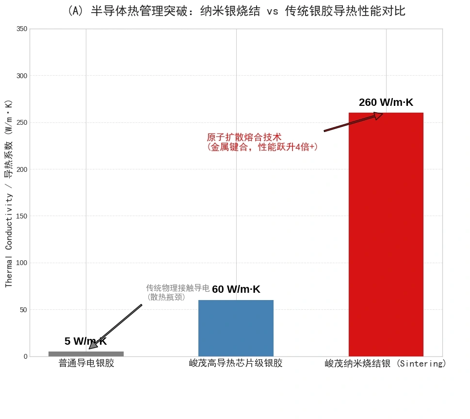
| Thermal conductivity (pressureless sintered silver) | 160–260 W/m·K | 30–60 W/m·K (solder) | ASTM D5470 |
| Tg | 110–195 °C | 80–120 °C | DMA / DSC |
| CTE | 26 ppm/°C | Above 50 ppm/°C | TMA |
| Die shear strength (gold-plated surface) | 16 MPa | 5–10 MPa | GB/T 7124 |
| Die-attach void rate | Below 5% (below 2% automotive) | 10–20% | C-SAM / X-ray |
| Cure shrinkage | Below 0.3% | 1–3% | ISO 2577 |
| Mobile ions (Na⁺/K⁺/Cl⁻) | Below 10 ppm | Above 50 ppm | IC ion chromatography |
| Shear retention after cycling (−40 to 125 °C, 500 cycles) | 84% | Marked decay | JESD22-A104 |
1. Why the Die-Attach Interface Is the First Yield Gate
Bottom line: die-attach failures rarely appear as immediate bond loss. They surface later as junction temperature drift, interfacial delamination, or open circuit, after thermal resistance and stress have degraded slowly in service. Judging whether a die-attach scheme is reliable means reading thermal, mechanical, and chemical channels on one table.
1.1 Decomposing Interface Thermal Resistance
Heat leaving the junction crosses a series of interfaces: the die-attach layer, the thermal interface material between die and lid, the interface between lid and heat sink, and the sink itself. Total junction-to-ambient budget on a high-power accelerator is typically only 0.25–0.5 °C/W, and the die-attach share splits into two tiers: 1–5 °C/W for filled epoxy systems and 0.1–0.5 °C/W for solder and sintered systems, close to an order of magnitude apart.
Die-attach thermal resistance equals bond line thickness divided by the product of thermal conductivity and effective contact area. Three variables govern the interface at the same time, and any one of them running out of control erases the advantage of the bulk material. The most common field error is buying a paste with a higher datasheet conductivity, then measuring a higher junction temperature because the bond line is thicker or the void content is higher.
SCITEO repeatedly observes in ASTM D5470 re-testing that the same formulation shifts with test pressure and bond line thickness. Acceptance testing should therefore fix the target pressure and target BLT, re-test thermal resistance, and combine it with C-SAM void rate and post-cycle drift instead of reading a single datasheet number.
1.2 Void Rate and Bond Line Thickness Criteria
Voids are the most direct failure source at the die-attach interface. A void conducts no heat, so heat flux is squeezed into the remaining contact area and local current density and temperature rise together; industry experience puts local junction temperature 10%–15% higher for every 10% of void area, which accelerates electromigration and dielectric breakdown over service life. Voids also act as stress concentrators, and cracks typically initiate at void edges.
Acceptance limits are tiered by application. Consumer and general industrial packages usually allow void area below 10%, high-reliability and automotive modules tighten to 5%, and military and high-power modules target 2% per MIL-STD-883 practice. Inspection relies on C-SAM and X-ray, because visual inspection cannot detect subsurface voids.
BLT control matters equally. Epoxy die attach typically lands at 15–30 μm, while solder and sintered layers reach 10–25 μm. Thinner layers mean lower thermal resistance, but they demand tighter dispensing consistency, die flatness, and pressure uniformity. SCITEO couples silver filler grading with rheology control to keep wet dispense weight and dot geometry inside a narrow band, so BLT stays reproducible at production takt.
2. Thermomechanical Reliability: Tg, CTE, and Shear Strength as One Set
Bottom line: no single metric predicts die-attach life. Silicon sits near 2.6 ppm/°C, SiC near 4.2 ppm/°C, aluminum nitride ceramic near 4.5 ppm/°C, and copper leadframes near 17 ppm/°C, so the die-attach modulus and CTE decide how stress is distributed between them.
2.1 Cure Shrinkage and Interfacial Residual Stress
Cure brings volume shrinkage. Excessive shrinkage leaves tensile residual stress at the interface, and die corners and the edges of large dies are where micro-cracks initiate first; too little shrinkage means insufficient physical anchoring and lower shear strength. A formulation has to satisfy both sides at once.
SCITEO's silver flake packing density design holds cure shrinkage below 0.3% (ISO 2577) while keeping volume resistivity at 3×10⁻⁵ Ω·cm (ASTM D257 and ASTM D2739) and shear strength high. CTE control lives in the same formulation: the chip-grade conductive silver adhesive holds CTE at 26 ppm/°C (TMA), so the layer expands in step with semiconductor and ceramic bodies and residual thermomechanical stress is reduced at the source, supporting large bare dies through −40 to 125 °C cycling.
2.2 Modulus Support Inside the Bonding Window
Wire bonding heats the substrate to 150–200 °C and adds ultrasonic energy. If the die attach has already passed its Tg at that point, the layer enters the rubbery state, storage modulus drops, ultrasonic energy is absorbed by the adhesive, and the effective power delivered to the bond interface falls short, showing up as low pull strength and poor bonding.
Tg marks the transition from a rigid glassy state to a soft rubbery state, so a higher Tg widens the window in which modulus keeps its structural role. SCITEO chip-grade conductive silver adhesive is offered across a 110–195 °C Tg range, holding high storage modulus inside the bonding window as a rigid base for gold or copper wire bonding, with 16 MPa die shear on gold-plated surfaces (GB/T 7124) and 84% shear retention after 500 cycles between −40 and 125 °C (TC500). On large dies, stress distributes in a gradient with higher shear concentration at the edges, which is why SCITEO optimizes filler grading and interfacial coupling in the same formula.
3. Sintered Interconnect: Process Boundaries of Pressureless Silver and Copper Sintering
Bottom line: once junction temperature passes 200 °C and power cycling enters the 100k range, polymer-based die attach reaches its material limit and sintering becomes the second mainline. Its value is not the conductivity figure but the fact that the bond no longer relies on a polymer matrix to carry heat and current.
3.1 Densification Path and Process Window Without Pressure
Silver sintering carries the conductive path with metal rather than resin: nano-silver and sub-micron silver particles diffuse atomically in a 200–250 °C window driven by surface energy, form necks between particles, and grow into a continuous silver skeleton. The finished bond returns to the bulk melting point of silver, about 961 °C, so the device stays structurally stable above any solder melting point, with thermal conductivity reaching 160–260 W/m·K (ASTM D5470) and volume resistivity down to 3×10⁻⁶ Ω·cm by four-point probe.
Process windows diverge. Conventional micron-silver sintering needs 5–40 MPa of assist pressure to close porosity, raising both equipment cost and die stress; nano and mixed nano/micro particle systems widen the window toward low pressure, and some formulations densify pressurelessly through a stepped profile that first holds at 110–140 °C to drive out organics and solvent, then ramps to peak. The stepped hold matters because solvent reaching its boiling point under the die center vents violently and leaves dense micro-voids directly beneath the die, which is why large dies need a longer pre-dry hold.
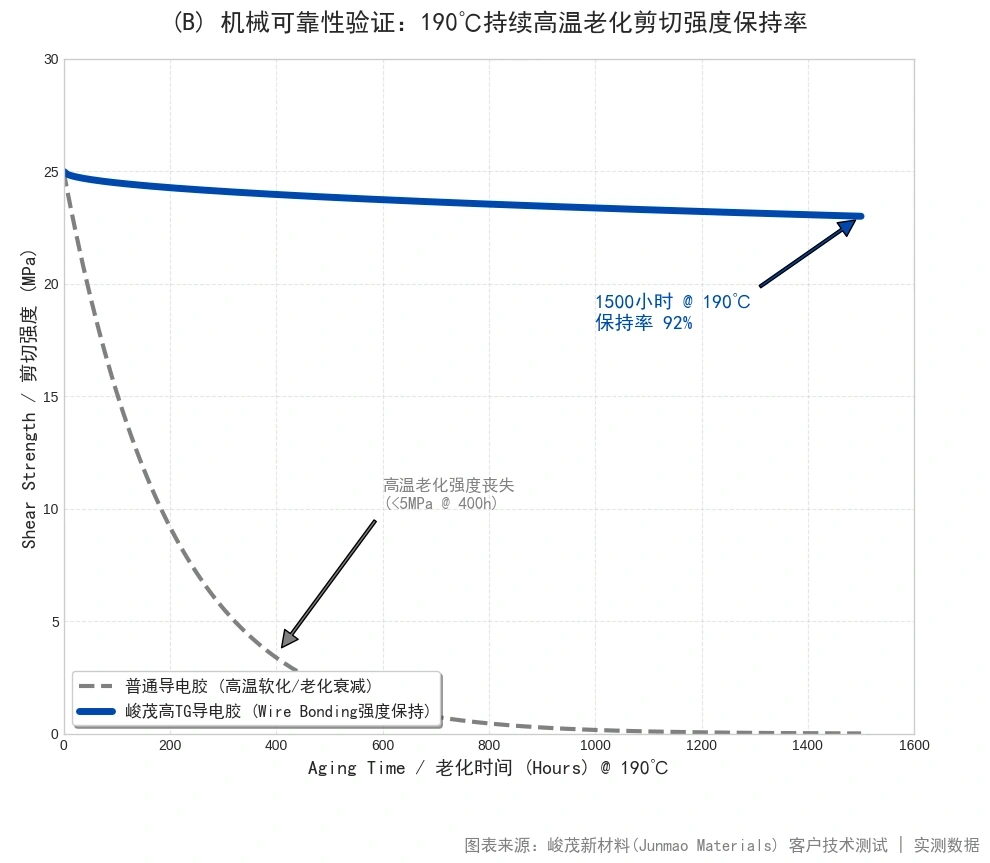
Shear strength for pressureless sintered silver exceeds 25 MPa after sintering above 200 °C and stays in the 20–25 MPa band after thermal cycling, 85/85, and continuous high-temperature aging. SCITEO supplies dedicated formulations for both pressure-assisted and pressureless routes and combines them by die area, line pressure capability, and void rate target.
3.2 Boundaries of Copper Sintering
Copper sintering answers two demands: cost and electrochemical reliability. Copper raw material is far cheaper than silver and intrinsically avoids silver's electrochemical migration and sulfide corrosion, at the price of oxidation control in the sintering atmosphere, which newer paste formulations solve by building anti-oxidation chemistry into the paste so that low-pressure and even air sintering become viable. On the thermomechanical side, sintered copper has higher yield strength and lower CTE mismatch against copper substrates, giving longer power-cycle life than sintered silver, which is why it is usually paired with double-sided cooling and copper clip structures.
4. Application Matrix: Four High-Value Die-Attach Interfaces
4.1 AI Heterogeneous Integration
Bottom line: as package size grows, shear load on the die attach scales with area and warpage moves from a secondary concern to a first-order constraint, so evaluation has to move from material level to package level.
Compute platforms now push single-accelerator thermal design power into the kilowatt range. Compute dies, high-bandwidth memory, and interposers are recombined as chiplets, package size advances from 5.5x reticle toward higher multiples, and panel-level packaging replaces round wafers with 510 mm-class rectangular panels, lifting area utilization from roughly 57% to 87%. With interface count multiplied, the thermal and stress budget left for each interface thins out.
Hybrid bonding pushes die-to-die interconnect density into the tens of thousands per square millimeter and shrinks bond pitch from 9 μm to 6 μm with 4.5 μm in development, but it addresses copper-to-copper connection between dies only. Between interposer and organic substrate, and between base die and carrier, a die-attach layer still has to provide mechanical retention and heat extraction. The thermal budget tightens as well: hybrid bonding anneals in a 150–400 °C window, so the die attach must cure beforehand and must not bleed or outgas during later high-temperature steps, while BLT on large dies is held near 25 μm or below to keep interface resistance low.
SCITEO's evaluation set for these large-area interfaces is a three-way test: C-SAM void rate, interface thermal resistance at target BLT, and package-level warpage together with post-cycle shear retention.
4.2 Automotive SiC Power Modules
Bottom line: automotive die attach faces rising junction temperature and accumulating power cycles at the same time, so modulus retention and interfacial fatigue matter as much as initial bond strength.
SiC traction inverters push junction temperature from the 150 °C ceiling of silicon devices to 175–205 °C, where lead-free solder approaches its melting range and creeps quickly, so die attach shifts from solder to pressureless sintered silver or high-Tg conductive silver adhesive rated for 300 °C. CTE mismatch is amplified in this setting: between a SiC die near 4.2 ppm/°C and a copper substrate near 17 ppm/°C, every power cycle becomes reciprocating shear stress in the die-attach layer, and when the layer cannot absorb it, micro-cracks initiate and thermal resistance climbs.
Acceptance is defined jointly by device and module standards: AEC-Q101 covers discrete stress qualification, module-level power cycling (PCsec) and thermal cycling cover interfacial fatigue, and JEDEC JESD22-A104 provides the common cycling method. SCITEO delivers a 110–195 °C Tg glassy-state window, 26 ppm/°C CTE, and above 16 MPa interfacial shear as one set of parallel indicators, holding 84% shear after TC500 between −40 and 125 °C.
4.3 Co-Packaged Optics and Laser Dies
Bottom line: co-packaged optics puts a high-temperature heat source and a temperature-sensitive device inside one package, so the die attach must be extremely low in void content and in cure displacement at the same time.
Co-packaged optics (CPO) integrates the optical engine and the switch ASIC on one substrate and shortens the electrical path from tens of centimeters to millimeters, at the cost of much harder thermal management. Switch ASIC power reaches the 750 W class on a die near 25 mm × 25 mm, heat flux approaches 120 W/cm², and junction temperature passes 120 °C easily, while an InP laser co-resident in the same package typically tolerates only about 70 °C before wavelength drift, power roll-off, and life degradation set in. Laser-related failures dominate optical module downtime statistics, and optical interconnect is advancing through 1.6T and 3.2T rates, so the pressure on this interface only increases.
Two requirements follow. Voids must be minimized, because a void concentrates heat flux into the remaining contact area, creating a local hotspot that translates directly into optical drift and catastrophic optical damage risk. Cure displacement must also be minimized, because cure shrinkage moves the die and disturbs sub-micron optical coupling. SCITEO approaches these interfaces with low-void dispensing formulations and low-shrinkage cure systems paired with a high-conductivity heat path, and controls total mass loss and volatile condensable materials per ASTM E595 so that volatiles do not condense on optical surfaces.
4.4 High-End Medical Imaging and Precision Intervention
Bottom line: medical devices move the die-attach criterion from conduction capability to long-term freedom from drift, and the sterilization, cleanliness, and regulatory requirements on the device side add a further rigid layer.
The imaging chain is moving toward modular tiling. Photon-counting spectral CT and long-axial PET/CT detectors pack a scintillator crystal array, light guide, silicon photomultiplier array, and dedicated front-end readout ASIC into a single detector module, then tile them axially and circumferentially into a detection surface on the 30 cm scale. Time-of-flight techniques push system timing resolution into the 190 picosecond range, crystal cutting reaches fine honeycomb-level dimensions, and readout electronics move from stitching general-purpose single-function chips to dedicated ASICs. The smaller the pixel, the more directly any positional or thermal shift writes itself into the reconstructed image. The die-attach layer therefore carries three jobs: extract heat from the readout chip to suppress dark current and gain drift, lock the crystal-to-photodetector alignment at the moment of cure, and hold flatness across the tiled surface. Integrated PET/MR adds a further requirement that the material introduce no magnetic trace impurities inside a strong magnetic field.
On the precision intervention side, the representative platforms are neurosurgical robots and MR-guided laser ablation. Stereotactic surgical robots reach sub-millimeter positioning accuracy, coordinating infrared optical tracking, a robotic arm, and control boards near a magnetic-field-free environment to place deep brain electrodes, perform biopsies, and evacuate hematomas. The matching intracranial depth, cortical, and thermocoagulation electrodes are invasive devices managed as Class III medical devices, and the brain-computer interface field already has dedicated classification and naming guidance in place, so ionic cleanliness and outgassing on the material side sit behind both hospital and regulatory thresholds. An MR-guided laser ablation system combines a semiconductor laser therapy unit with a single-use laser fiber kit, using proton resonance thermometry to hold the ablation core between 60 and 90 °C with measurement error below 1 °C through a 3 mm burr hole. On that chain, the laser chip attach interface directly sets output power stability and temperature control accuracy, while the fiber coupling module must not shift or outgas after cure.
Sterilization and cleanliness requirements are equally rigid. Single-use instruments are typically sterilized with ethylene oxide (in the spirit of ISO 11135) or gamma irradiation (ISO 11137, with a typical minimum dose of 25 kGy), and reusable instruments must also survive high-temperature steam. Irradiation drives chain scission and crosslinking in polymers, while ethylene oxide requires that no mobile hazardous residue remains after aeration. The device-level biological evaluation is completed by the device maker under the ISO 10993 series, and the material side is expected to deliver quantified data on low outgassing, low ion migration, and interfacial strength retention after sterilization.
On the material side, SCITEO supplies two grades of chip-grade conductive silver adhesive for these two chains: a low-outgassing low-ionic grade that supports detector tiling and robot control modules with CVCM below 0.05% after cure, tiled-surface flatness held within 5 μm, and above 90% shear retention after 25 kGy irradiation, and a high-thermal-conductivity low-stress grade that supports laser chip attach and fine deep-electrode interconnect with thermal conductivity in the 40 W/m·K class and void rate below 3%, both offering an 80–100 °C low-temperature cure window to protect heat-sensitive optical and polymer components.
5. Ionic Purity and High-Throughput Process Fit
5.1 Mobile Ions and Halogen-Free Thresholds
Bottom line: ion and halogen control is not a secondary anti-delamination metric, but the condition that determines how long insulation performance survives under damp-heat bias.
The die-attach layer sits directly against die and substrate, making it the most direct transport path for ions under humidity and bias. Chloride, sodium, and potassium residues from epoxy synthesis act as electrolytes, accelerate anodic dissolution of silver, and drive silver ions toward the cathode where they reduce into dendrites; once a dendrite bridges two electrodes, the short circuit is irreversible. Migration also drives conductive anodic filament (CAF) growth and degrades insulation on fine-pitch routing. The common industry limit for high-reliability encapsulants is mobile ion content below 10 ppm by IC ion chromatography.
Halogen-free requirements are tightening in parallel. IEC 61249-2-21 defines halogen-free material as chlorine below 900 ppm, bromine below 900 ppm, and total halogen below 1500 ppm, and automotive and export markets are enforcing that definition more strictly. SCITEO semiconductor-grade conductive silver adhesive uses electronic-grade purified resin and surface-passivated silver flakes, reducing active ions below 10 ppm through repeated deionized water washing and molecular distillation, and uses a low-moisture-absorption resin backbone to cut off the water path into the layer, showing no dendrite growth after HAST under 100 V bias.
5.2 Dispensing Rheology at Production Takt
Bottom line: die-attach yield on an automated line is set by how the rheological structure matches takt, and tailing, slumping, and needle clogging all map to measurable rheology parameters.
When the needle lifts at high speed, an adhesive whose cohesion is lower than its adhesion, or whose viscosity recovers too slowly, pulls a thin filament that can fall across the bond pad and contaminate the wire-bonding area, degrading bond strength. Insufficient yield stress produces slumping and flow, which risks shorts on narrow-pitch pads. The answer is thixotropic structure: a shear-thinning system drops viscosity under the high shear inside the needle, dispenses smoothly, then recovers viscosity within milliseconds once shear is removed, breaking the filament cleanly. For thick-film coating and large-die bonding, high yield stress preserves dot geometry and BLT before cure.
SCITEO tunes rheology additives together with silver filler grading to hold viscosity recovery and the thixotropic loop inside the process window, so continuous dispensing runs on 25G precision needles without clogging or tailing and works with both jetting and stencil printing. Natural thawing of refrigerated paste is part of the same production discipline: incomplete thawing condenses atmospheric moisture into the adhesive, forming voids under the die and disrupting the cure network.
6. Die-Attach Selection Quick Reference
| Application | Typical failure mode | Primary criterion | SCITEO direction |
|---|---|---|---|
| AI heterogeneous integration and panel-level packaging | Large-die warpage, interfacial delamination | Low CTE, low cure shrinkage, interface resistance at target BLT | Chip-grade conductive silver adhesive (high-Tg, low-CTE grades) |
| Automotive SiC power modules | Interfacial shear fatigue under power cycling | Tg and modulus retention, CTE, sintered-layer void rate | Pressureless sintered silver and high-Tg conductive silver adhesive |
| Co-packaged optics and laser dies | Optical drift and catastrophic optical damage from void hotspots | Low void rate, low cure shrinkage, low outgassing | Low-void conductive silver adhesive and sintered silver |
| Medical imaging detector arrays | Dark current rise and gain drift from void hotspots | Low void rate, low interface resistance, CVCM below 0.05%, tiled-surface flatness | Low-outgassing low-ionic conductive silver adhesive |
| Neurosurgical robots and intracranial electrodes | Fine interconnect open circuit, interfacial degradation after sterilization | Sterilization compatibility, low ions, low outgassing, low-temperature cure window | Low-stress low-outgassing grade and low-temperature cure grade |
| Laser ablation and fiber coupling modules | Output power and temperature-control drift from void hotspots | 40 W/m·K class thermal conductivity, void rate below 3%, low cure displacement | High-thermal-conductivity low-stress conductive silver adhesive |
7. Conclusion
Die attach is the most underrated step in the packaging chain: it decides whether heat can leave the junction and whether current can reach the next interface with low loss. As AI heterogeneous integration, automotive SiC power modules, co-packaged optics, and medical imaging with precision intervention push interface loads to new levels, die-attach evaluation is shifting from single-point parameters to an evidence matrix in which interface thermal resistance, void rate, Tg, CTE, cure shrinkage, mobile ions, and post-cycle shear retention must all hold. Any missing item surfaces as a failure in volume production.
SCITEO covers the range from 5–60 W/m·K and 3×10⁻⁵ Ω·cm to 160–260 W/m·K and 3×10⁻⁶ Ω·cm with two routes, chip-grade epoxy conductive silver adhesive and pressureless sintered silver, and supports advanced packaging die attach with a formulation platform built on low ionic content, low cure shrinkage, low stress, and sterilization compatibility, backed by batch consistency and traceability documentation for medical, automotive, and compute customers. As power density keeps rising and cleanliness thresholds keep tightening, SCITEO keeps defining material boundaries with first-party reproducible data, delivering verifiable and iterable interface solutions.
This article is SCITEO Advanced Materials original technical content; unauthorized reproduction is prohibited.
Appendix: Process & Engineering Adhesive FAQ Index
For large dies above 10 × 10 mm, how do you bring void rate and warpage down at the same time?
The hard part on a large die is the longer outgassing path. Solvent and low-molecular-weight volatiles must diffuse from the die center to the edge, so the longer that path, the more micro-voids remain near the center; at the same time, CTE difference between die and substrate accumulates with area, and warpage changes the bond line thickness distribution. Three actions are normally taken together: switch the dispense pattern to a grid or cross-with-perimeter so no closed cavity traps gas; use a stepped cure that holds at 110–140 °C to drive volatiles out smoothly before ramping to the crosslinking peak; and re-match tooling and pressure parameters to substrate thickness and area. Acceptance relies on C-SAM and X-ray, with automotive modules holding void area below 2% and general industrial packages below 5%. SCITEO stabilizes wet bond line thickness on these interfaces through filler grading and rheology control, so dispense weight and dot geometry variation do not amplify into voids.
Does die-attach conductive adhesive still have a role once hybrid bonding scales?
They solve connection problems at different levels. Hybrid bonding forms copper-to-copper and dielectric-to-dielectric bonds directly at atomic scale between dies, pushing interconnect density into the tens of thousands per square millimeter and shrinking pitch from 9 μm to 6 μm with 4.5 μm in development. Between interposer and organic substrate, and between base die and carrier, a die-attach layer must still provide mechanical retention and heat extraction, and hybrid bonding cannot replace it. The tighter constraint is thermal budget: hybrid bonding anneals in a 150–400 °C window, so the die attach must cure beforehand and must not bleed or outgas during later high-temperature steps. Die-attach adhesive is therefore not displaced but pushed toward higher cleanliness and a narrower process window.
How should interface thermal resistance be accepted, and why is thermal conductivity alone not enough?
Because interface resistance is set by conductivity, bond line thickness, and effective contact area together, expressed as BLT divided by the product of conductivity and effective contact area. The same formulation can measure several times higher resistance at a thicker bond line or a different applied pressure. Total junction-to-ambient budget on a high-power accelerator is often only 0.25–0.5 °C/W, with the die-attach share at 1–5 °C/W for filled epoxy and 0.1–0.5 °C/W for solder and sintered systems, and that order-of-magnitude difference sets the junction temperature margin. The engineering method is to re-test resistance per ASTM D5470 at the target pressure and target BLT, then judge it together with C-SAM void rate and post-cycle resistance drift instead of reading a single datasheet conductivity value.
When dispensing speed goes up, why do tailing and slumping appear: the adhesive or the line?
Usually it is a mismatch between rheological structure and takt. At the instant the needle lifts, an adhesive whose cohesion is below its adhesion, or whose viscosity recovers too slowly, pulls a thin filament that can fall across the pad and contaminate the bonding area. Insufficient yield stress produces slumping and flow, which risks shorts on narrow-pitch pads. The measurable criteria are thixotropic loop area and viscosity recovery after shear removal, and a shear-thinning system must recover within milliseconds for clean filament break. SCITEO tunes rheology additives with silver filler grading to combine high yield stress with fast recovery, supporting continuous dispensing on 25G precision needles, jetting, and stencil printing while holding dot geometry on thick-film and large-die bonding.
Why are void rate and outgassing so critical for laser die attach in co-packaged optics?
Because one package contains both a high-temperature heat source and a temperature-sensitive device. Switch ASIC power reaches the 750 W class at a heat flux approaching 120 W/cm², and junction temperature passes 120 °C easily, while an InP laser typically tolerates only about 70 °C before wavelength drift, power roll-off, and life degradation. A void in the die-attach layer squeezes heat flux into the remaining contact area, creating a local hotspot that turns directly into optical performance drift, and cure shrinkage displaces the die and disturbs sub-micron optical coupling. The criteria for these interfaces are therefore low void rate, low cure shrinkage, and low outgassing in parallel, with total mass loss and volatile condensable materials controlled per ASTM E595 so volatiles do not condense on optical surfaces.
What do high-end medical imaging and precision intervention devices require from conductive adhesive that consumer electronics do not?
The differences concentrate in three areas. First, long-term baseline stability: photon-counting spectral CT and long-axial PET/CT detectors pack a crystal array, light guide, silicon photomultiplier, and dedicated front-end readout ASIC into one module, with system timing resolution already in the 190 picosecond range, so voids in the die-attach layer create local heat buildup whose thermal drift converts directly into rising dark current and gain drift and shows up as artifacts in the reconstructed image. On the intervention side, deep-electrode fine interconnect and laser chip attach interfaces must also hold their performance without drift, and these devices tolerate far lower void area and interface resistance than industrial packaging. Second, sterilization compatibility: single-use instruments are typically sterilized with ethylene oxide (in the spirit of ISO 11135) or gamma irradiation (ISO 11137, typically from 25 kGy), so the adhesive must retain shear strength, insulation performance, and ionic cleanliness after irradiation-induced chain scission and after ethylene oxide aeration. Third, verifiable cleanliness data: the biological evaluation belongs to the device maker under the ISO 10993 series, invasive electrodes are managed as Class III medical devices, and the material side is expected to supply quantified low-outgassing and low-ion-migration data. SCITEO addresses these requirements with a formulation strategy built on four parallel attributes: low stress, low moisture absorption, low outgassing, and low ions.
How should acceptance thresholds for mobile ions and halogen content be set?
Start from the failure path, then set the number. The die-attach layer sits directly against die and substrate and is the most direct ion transport path under humidity and bias: chloride, sodium, and potassium act as electrolytes, accelerate anodic dissolution of silver, and drive silver ions to the cathode where they deposit as dendrites; a bridging dendrite causes irreversible short circuit and also drives conductive anodic filament growth. The common industry threshold for high-reliability encapsulants is mobile ion content below 10 ppm by IC ion chromatography, and the halogen-free reference is IEC 61249-2-21, with chlorine and bromine each below 900 ppm and total halogen below 1500 ppm. SCITEO semiconductor-grade conductive silver adhesive uses electronic-grade purified resin and surface-passivated silver flakes, holding active ions below 10 ppm after repeated deionized water washing and molecular distillation, with no dendrite growth after HAST under 100 V bias.